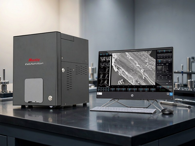
Easynano Scan Benchtop Scanning Electron Microscope
Model: Easynano ScanA benchtop scanning electron microscope with a compact footprint that needs no dedicated room and only simple sample preparation. Suited to surface morphology and high-magnification structural analysis of materials, geological and biological samples, it sits between optical microscopy and a full-size SEM.
Specifications
| Type | Benchtop all-in-one scanning electron microscope, high/low vacuum dual mode |
|---|---|
| Resolution | 5nm |
| Magnification | Up to 200,000x |
| Sample stage | XYZ motorized sample stage |
| Imaging | Autofocus and stigmation correction, multiple imaging modes |
| Vacuum system | Fast switching between high/low vacuum |
| Accessories | Optional energy-dispersive X-ray spectrometer (EDX) and vacuum ion sputter coater |
| Software | Measurement and analysis, remote diagnostics, free upgrades |
| Structure | All-in-one desktop design with a small footprint |
| Applications | Materials science, automotive and metals, energy, semiconductors and electronics |
Features
- Benchtop all-in-one design, requiring no dedicated electron microscopy room
- High/low vacuum dual mode, adapting to various samples
- 5nm high resolution, up to 200,000x magnification
- Autofocus and stigmation correction for stable imaging
- XYZ motorized sample stage for convenient operation
- Can be equipped with an EDX spectrometer for micro-morphology plus composition analysis
- Free software upgrades with remote diagnostics support
Applications
- Materials science and microstructure analysis
- Failure analysis of metallic materials
- Inspection of semiconductors and electronic devices
- Energy materials research
- Quality inspection of automotive parts
Frequently Asked Questions
How is a benchtop SEM different from a full-size one?
It is small, needs no dedicated room, and works much like put-the-sample-in-and-image. Resolution and depth of field still far exceed optical microscopy, which suits routine morphology and rapid screening.
Do samples need preparation?
Conductive samples can be imaged directly. Non-conductive samples need coating, or low-vacuum mode to reduce charging.
What can it image?
Fracture surfaces and inclusions in metals, powder morphology and particle size, coating cross sections, fibre surfaces and micro/nano structures. With EDS it also gives elemental composition.
How should it work alongside an optical microscope?
Use the optical microscope for quick location and overview, then move to the SEM for detail. That combination is the most efficient.
Want the full specification sheet?
Leave a number and we will send the specification sheet and a quotation for the Easynano Scan Benchtop Scanning Electron Microscope. Calls returned within 10 minutes on working days.